- 您现在的位置:买卖IC网 > Sheet目录340 > MAX16821CATI+T (Maxim Integrated)IC LED DRIVR HIGH BRIGHT 28-TQFN
�� �
�
�High-Power� Synchronous� HBLED�
�Drivers� with� Rapid� Current� Pulsing�
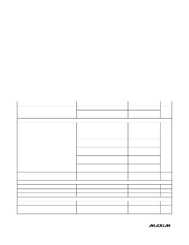
�ABSOLUTE� MAXIMUM� RATINGS�
�IN� to� SGND.............................................................-0.3V� to� +30V�
�BST� to� SGND..........................................................-0.3V� to� +35V�
�BST� to� LX..................................................................-0.3V� to� +6V�
�DH� to� LX� ...........................................-0.3V� to� (V� BST� -� V� LX� )� +� 0.3V�
�DL� to� PGND................................................-0.3V� to� (V� DD� +� 0.3V)�
�V� CC� to� SGND............................................................-0.3V� to� +6V�
�V� CC� ,� V� DD� to� PGND� ...................................................-0.3V� to� +6V�
�SGND� to� PGND� .....................................................-0.3V� to� +0.3V�
�All� Other� Pins� to� SGND...............................-0.3V� to� (V� CC� +� 0.3V)�
�Continuous� Power� Dissipation� (T� A� =� +70°C)�
�28-Pin� TQFN� 5mm� x� 5mm� (derate� 34.5mW/°C�
�above� +70°C)� ............................................................2758mW�
�Operating� Temperature� Range� .........................-40°C� to� +125°C�
�Junction� Temperature� ......................................................+150°C�
�Storage� Temperature� Range� .............................-65°C� to� +150°C�
�Lead� Temperature� (soldering,� 10s)� .................................+300°C�
�V� CC� Current� ......................................................................300mA�
�Stresses� beyond� those� listed� under� “Absolute� Maximum� Ratings”� may� cause� permanent� damage� to� the� device.� These� are� stress� ratings� only,� and� functional�
�operation� of� the� device� at� these� or� any� other� conditions� beyond� those� indicated� in� the� operational� sections� of� the� specifications� is� not� implied.� Exposure� to�
�absolute� maximum� rating� conditions� for� extended� periods� may� affect� device� reliability.�
�ELECTRICAL� CHARACTERISTICS�
�(V� CC� =� 5V,� V� DD� =� V� CC� ,� T� A� =� T� J� =� -40°C� to� +125°C,� unless� otherwise� noted.� Typical� values� are� at� T� A� =� +25°C.)� (Note� 1)�
�PARAMETER�
�SYMBOL�
�CONDITIONS�
�MIN�
�TYP�
�MAX�
�UNITS�
�Input-Voltage� Range�
�Quiescent� Supply� Current�
�V� IN�
�I� Q�
�Internal� LDO� on�
�Internal� LDO� off� (V� CC� connected� to� V� IN� )�
�V� EN� =� V� CC� or� SGND,� no� switching�
�7�
�4.75�
�2.7�
�28�
�5.50�
�5.5�
�V�
�mA�
�LED� CURRENT� REGULATOR�
�V� IN� =� V� CC� =� 4.75V� to� 5.5V,� f� SW� =� 500kHz�
�(MAX16821A)�
�V� IN� =� 7V� to� 28V,� f� SW� =� 500kHz�
�(MAX16821A)�
�0.594�
�0.594�
�0.600�
�0.600�
�0.606�
�0.606�
�Differential� Set� Value�
�(V� SENSE� +� to� V� SENSE-� )� (Note� 2)�
�Soft-Start� Time�
�t� SS�
�V� IN� =� V� CC� =� 4.75V� to� 5.5V,� f� SW� =� 500kHz�
�(MAX16821B)�
�V� IN� =� 7V� to� 28V,� f� SW� =� 500kHz�
�(MAX16821B)�
�V� IN� =� V� CC� =� 4.75V� to� 5.5V,� f� SW� =� 500kHz�
�(MAX16821C)�
�V� IN� =� 7V� to� 28V,� f� SW� =� 500kHz�
�(MAX16821C)�
�0.098�
�0.098�
�0.028�
�0.028�
�0.100�
�0.100�
�0.030�
�0.030�
�1024�
�0.102�
�0.102�
�0.032�
�0.032�
�V�
�Clock�
�Cycles�
�STARTUP/INTERNAL� REGULATOR�
�V� CC� Undervoltage� Lockout� (UVLO)�
�UVLO�
�V� CC� rising�
�4.1�
�4.3�
�4.5�
�V�
�UVLO� Hysteresis�
�V� CC� falling�
�200�
�mV�
�V� CC� Output� Voltage�
�V� IN� =� 7V� to� 28V,� I� SOURCE� =� 0� to� 60mA�
�4.85�
�5.10�
�5.30�
�V�
�MOSFET� DRIVER�
�Output� Driver� Impedance�
�Output� Driver� Source/Sink� Current�
�I� DH� ,� I� DL�
�Low� or� high� output,� I� SOURCE/SINK� =� 20mA�
�1.1�
�4�
�3�
�?�
�A�
�Nonoverlap� Time�
�t� NO�
�C� DH/DL� =� 5nF�
�35�
�ns�
�2�
�_______________________________________________________________________________________�
�发布紧急采购,3分钟左右您将得到回复。
相关PDF资料
MAX16822AASA/V+
IC LED DRIVER HIGH BRIGHT 8SOIC
MAX16826ATJ+C24
IC LED DVR HB PROGR 32-HQFN
MAX16835ATE+T
IC LED DRIVR HIGH BRIGHT 16-TQFN
MAX16838AUP+
IC LED DRIVR HIGH BRIGHT 20TSSOP
MAX1698EUB
IC LED DRVR WT/CLR BCKLGT 10MSOP
MAX17014EVKIT+
KIT EVAL FOR MAX17014
MAX17061AETI+T
IC LED DRVR WHITE BCKLGT 28-TQFN
MAX17061ETI+T
IC LED DRVR WHITE BCKLGT 28-TQFN
相关代理商/技术参数
MAX16821EVKIT+
制造商:Maxim Integrated Products 功能描述:HIGH-POWER SYNCHRONOUS HBLED DRIVER - Boxed Product (Development Kits)
MAX16822AASA/V+
功能描述:LED照明驱动器 2MHz HB w/MOSFET & HSide Crnt Sense RoHS:否 制造商:STMicroelectronics 输入电压:11.5 V to 23 V 工作频率: 最大电源电流:1.7 mA 输出电流: 最大工作温度: 安装风格:SMD/SMT 封装 / 箱体:SO-16N
MAX16822AASA/V+T
功能描述:LED照明驱动器 2MHz HB w/MOSFET & HSide Crnt Sense RoHS:否 制造商:STMicroelectronics 输入电压:11.5 V to 23 V 工作频率: 最大电源电流:1.7 mA 输出电流: 最大工作温度: 安装风格:SMD/SMT 封装 / 箱体:SO-16N
MAX16822AASA+
功能描述:LED照明驱动器 2MHz HB w/MOSFET & HSide Crnt Sense RoHS:否 制造商:STMicroelectronics 输入电压:11.5 V to 23 V 工作频率: 最大电源电流:1.7 mA 输出电流: 最大工作温度: 安装风格:SMD/SMT 封装 / 箱体:SO-16N
MAX16822AASA+T
功能描述:LED照明驱动器 2MHz HB w/MOSFET & HSide Crnt Sense RoHS:否 制造商:STMicroelectronics 输入电压:11.5 V to 23 V 工作频率: 最大电源电流:1.7 mA 输出电流: 最大工作温度: 安装风格:SMD/SMT 封装 / 箱体:SO-16N
MAX16822BASA+
功能描述:LED照明驱动器 2MHz HB w/MOSFET & HSide Crnt Sense RoHS:否 制造商:STMicroelectronics 输入电压:11.5 V to 23 V 工作频率: 最大电源电流:1.7 mA 输出电流: 最大工作温度: 安装风格:SMD/SMT 封装 / 箱体:SO-16N
MAX16822BASA+T
功能描述:LED照明驱动器 2MHz HB w/MOSFET & HSide Crnt Sense RoHS:否 制造商:STMicroelectronics 输入电压:11.5 V to 23 V 工作频率: 最大电源电流:1.7 mA 输出电流: 最大工作温度: 安装风格:SMD/SMT 封装 / 箱体:SO-16N
MAX16822BEVKIT+
功能描述:LED 照明开发工具 MAX16822B Eval Kit RoHS:否 制造商:Fairchild Semiconductor 产品:Evaluation Kits 用于:FL7732 核心: 电源电压:120V 系列: 封装: